Market Overview
The US extreme ultraviolet lithography (EUV) systems market has gained significant traction in recent years as the semiconductor industry continues to drive towards smaller, more advanced chip geometries. EUV lithography is a cutting-edge technology that utilizes extremely short-wavelength light (approximately 13.5 nanometers) to enable the fabrication of integrated circuits with feature sizes as small as 10 nanometers or less. This revolutionary technology is poised to replace conventional deep ultraviolet (DUV) lithography, which has reached its practical limits in supporting the industry’s relentless pursuit of Moore’s Law.
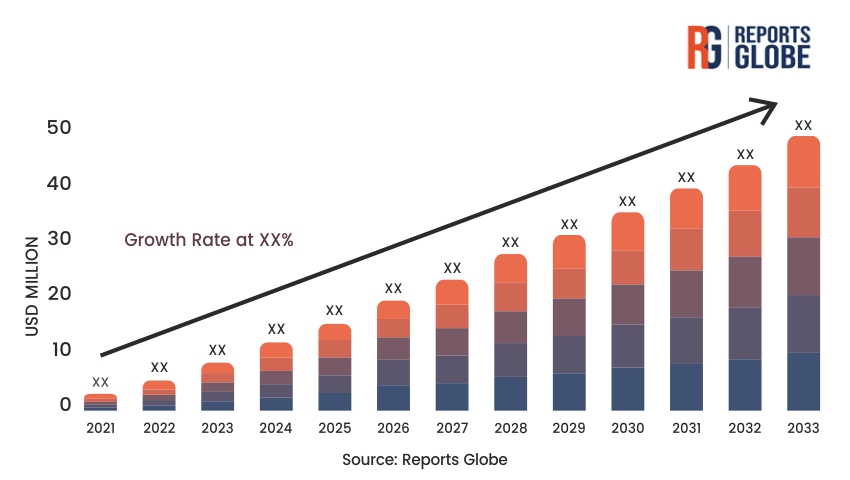
The US EUV systems market was valued at approximately $1.8 billion in 2022 and is expected to grow at a compound annual growth rate (CAGR) of around 20% from 2023 to 2028. This growth is driven by the increasing demand for advanced semiconductor devices, the continuous scaling of integrated circuits, and the critical role of EUV lithography in enabling the next generation of chip manufacturing.
The market is dominated by a few key players, including ASML Holding N.V., Nikon Corporation, and Carl Zeiss AG, who have been at the forefront of developing and commercializing EUV lithography systems. These systems are primarily used in state-of-the-art semiconductor fabrication facilities, known as fabs, to produce the most advanced logic and memory chips for a wide range of applications, from consumer electronics to data centers and high-performance computing.
Key Takeaways of the market
- The US EUV systems market is experiencing rapid growth, driven by the semiconductor industry’s relentless pursuit of smaller, more advanced chip geometries.
- EUV lithography is a transformative technology that enables the fabrication of integrated circuits with feature sizes as small as 10 nanometers or less.
- The market is highly concentrated, with a few leading players dominating the landscape and investing heavily in EUV technology development.
- Significant investments in R&D, complex manufacturing processes, and the high cost of EUV systems pose significant barriers to entry for new players.
- Ongoing technological advancements, such as improvements in light source power, mask handling, and metrology, are crucial to driving the adoption of EUV lithography.
- Collaboration between equipment manufacturers, semiconductor fabs, and research institutions is essential for driving the ecosystem and addressing technical challenges.
- Regulatory requirements and standards, as well as the availability of skilled workforce, are important factors shaping the market dynamics.
Market Drivers
The primary driver of the US EUV systems market is the semiconductor industry’s relentless pursuit of Moore’s Law, which has been the guiding principle for the continuous scaling and performance improvement of integrated circuits. As the industry transitions to smaller process nodes, traditional DUV lithography has reached its practical limits, and EUV lithography has emerged as the solution to enable the fabrication of ever-smaller features on semiconductor chips.
The increasing demand for advanced semiconductor devices, particularly in the areas of high-performance computing, artificial intelligence, 5G communication, and data centers, has fueled the need for more powerful and energy-efficient chips. EUV lithography is crucial in enabling the production of these cutting-edge semiconductors, as it allows for the creation of denser and more complex integrated circuits, ultimately driving the growth of the US EUV systems market.
Furthermore, the growing importance of semiconductor technology in a wide range of applications, from consumer electronics to industrial and automotive sectors, has increased the overall demand for advanced chip manufacturing capabilities. EUV lithography, with its ability to produce smaller, faster, and more energy-efficient chips, has become a strategic imperative for leading semiconductor manufacturers to maintain their competitive edge and meet the evolving market demands.
Additionally, the continuous investment and collaboration between equipment manufacturers, semiconductor fabs, and research institutions have played a significant role in driving the development and adoption of EUV lithography technology in the US market.
Market Restraints
One of the key restraints in the US EUV systems market is the high cost and complexity associated with the development, manufacturing, and deployment of these advanced lithography systems. EUV lithography requires specialized and highly precise equipment, as well as a meticulously controlled manufacturing environment to ensure the proper functioning of the systems.
The high capital expenditure required for the acquisition and installation of EUV systems, which can range from hundreds of millions to over a billion dollars per fab, can be a significant barrier for some semiconductor manufacturers, particularly smaller or more resource-constrained companies. This high cost can limit the broader adoption of EUV lithography and create a competitive advantage for larger, well-capitalized players in the market.
Additionally, the technical challenges associated with EUV lithography, such as the development of high-power light sources, the optimization of mask handling, and the advancement of metrology and inspection capabilities, have posed significant hurdles for equipment manufacturers. Overcoming these technical barriers requires substantial R&D investments and collaboration across the industry ecosystem.
The availability of skilled workforce capable of operating and maintaining these complex EUV systems is another restraint. The specialized nature of EUV lithography requires highly trained personnel, and the limited pool of experienced technicians and engineers can hamper the industry’s ability to scale up EUV-based manufacturing.
Regulatory requirements and industry standards also play a role in shaping the market dynamics. Compliance with stringent safety and environmental regulations, as well as the need to adhere to industry-wide standards, can add complexity and cost to the adoption of EUV lithography.
Market Opportunity
The US EUV systems market presents several promising opportunities for market players. As semiconductor manufacturers continue to push the boundaries of chip scaling and performance, the demand for EUV lithography is expected to grow significantly in the coming years.
One key opportunity lies in the ongoing technological advancements in EUV systems, which can lead to improvements in critical areas such as light source power, mask handling, and metrology. Manufacturers that successfully develop and commercialize more efficient, reliable, and cost-effective EUV systems will be well-positioned to capitalize on the growing market demand.
Additionally, the expansion of EUV lithography beyond the leading-edge logic and memory chip production, into other semiconductor applications like power electronics, analog/mixed-signal, and specialized devices, presents an opportunity for market growth. As the technology matures and the cost-benefit equation becomes more favorable, EUV lithography could find adoption in a wider range of semiconductor manufacturing processes.
The increasing emphasis on environmentally sustainable manufacturing practices also presents an opportunity for EUV systems, as the technology can potentially offer advantages in terms of reduced energy consumption and waste generation compared to conventional lithography methods.
Furthermore, the ongoing collaboration between equipment manufacturers, semiconductor fabs, and research institutions, such as universities and government-funded research centers, can lead to the development of innovative solutions and the creation of a robust EUV ecosystem. This collaborative approach can help address technical challenges, drive technological advancements, and ultimately expand the market opportunities for EUV lithography in the US.
Market Segment Analysis
Logic Chip Segment: The logic chip segment is the largest and most crucial application area for EUV lithography in the US market. Logic chips, which are the core components of modern computing and communication devices, require the most advanced process nodes and feature sizes to achieve the desired performance, power efficiency, and functionality.
EUV lithography has become an essential technology for the fabrication of leading-edge logic chips, enabling the production of integrated circuits with feature sizes as small as 10 nanometers or even below. Semiconductor manufacturers, such as Intel, NVIDIA, and AMD, have been at the forefront of adopting EUV technology to maintain their competitive edge and meet the growing demand for high-performance computing and AI applications.
The logic chip segment is expected to continue driving the growth of the US EUV systems market, as semiconductor companies invest heavily in the development and scaling of their advanced logic processes. The increasing importance of cutting-edge logic chips in emerging technologies, such as 5G, autonomous vehicles, and cloud computing, is further fueling the demand for EUV lithography in this segment.
Memory Chip Segment: The memory chip segment is another key application area for EUV lithography in the US market. Memory chips, including DRAM and NAND flash, are critical components in a wide range of electronic devices, from smartphones to data centers, and their performance and capacity requirements have been steadily increasing.
EUV lithography has become essential for the fabrication of high-density and high-performance memory chips, enabling the production of smaller, more power-efficient, and higher-capacity memory devices. Leading memory chip manufacturers, such as Samsung, SK Hynix, and Micron, have been adopting EUV technology to maintain their competitive edge and meet the growing demand for advanced memory solutions.
The memory chip segment is expected to contribute significantly to the growth of the US EUV systems market, driven by the continuous need for increased memory capacity and performance in a wide range of applications, from consumer electronics to data centers and cloud computing. As the industry transitions to newer memory technologies, such as 3D NAND and emerging memory architectures, the importance of EUV lithography in the memory chip segment is likely to increase further.
Regional Analysis
The US EUV systems market is primarily concentrated in the Southwestern and Western regions of the country, particularly in areas with a significant presence of semiconductor manufacturing facilities and research institutions.
The Southwestern region, which includes states like Texas and Arizona, has been a major hub for the US semiconductor industry, with several major fabs and research centers located in the area. The region’s favorable business climate, availability of skilled workforce, and established infrastructure have contributed to the growth of the EUV systems market in this region.
The Western region, encompassing states like California and Oregon, has also been a significant contributor to the US EUV systems market. This region is home to leading semiconductor companies, such as Intel and NVIDIA, as well as renowned research institutions like the University of California and the Lawrence Berkeley National Laboratory, which have been at the forefront of EUV lithography research and development.
The Northeastern and Midwestern regions of the US have also witnessed increased activity in the EUV systems market, though to a lesser extent compared to the Southwestern and Western regions. The presence of semiconductor manufacturers and research facilities, as well as the growing emphasis on advanced manufacturing and innovation in these regions, have contributed to the market’s expansion.
Overall, the regional dynamics in the US EUV systems market reflect the concentration of the semiconductor industry and the emphasis on advanced manufacturing and technological innovation. Manufacturers and industry stakeholders continue to monitor regional trends, infrastructure development, and the availability of skilled talent to strategically position their EUV lithography offerings and capture the growing market opportunities.
Competitive Analysis
The US EUV systems market is dominated by a few key players who have been at the forefront of developing and commercializing advanced EUV lithography technology. These players include ASML Holding N.V., Nikon Corporation, and Carl Zeiss AG.
ASML Holding N.V. is the undisputed market leader, with its EUV systems accounting for the majority of the US market share. The company has been a pioneer in EUV lithography, investing heavily in R&D and collaborating extensively with semiconductor manufacturers and research institutions to drive the technology’s development and adoption.
Nikon Corporation, a Japanese multinational corporation, has also been a significant player in the US EUV systems market. The company has leveraged its expertise in optical technologies and semiconductor manufacturing equipment to develop and commercialize its own EUV lithography solutions.
Carl Zeiss AG, a German optics and opto-electronics company, is another key player in the US EUV systems market. The company’s expertise in high-precision optical components and metrology has enabled it to play a crucial role in the development and integration of critical EUV subsystems.
While these three players dominate the market, there are also a few smaller, specialized companies that have carved out niche positions by offering unique EUV-related products and services, such as mask blank production, metrology tools, and inspection systems.
The competitive landscape in the US EUV systems market is characterized by high barriers to entry, driven by the significant investments required for R&D, manufacturing capabilities, and the need for extensive collaboration across the industry ecosystem. The leading players have leveraged their technical expertise, financial resources, and strategic partnerships to maintain their competitive advantage and stay ahead of the curve in the constantly evolving EUV lithography landscape.
Key Industry Developments
- Continuous advancements in EUV light source power, improving the throughput and cost-effectiveness of EUV lithography systems.
- Improvements in mask handling and defect inspection capabilities, enhancing the yield and reliability of EUV-based manufacturing.
- Development of advanced metrology and process control technologies to enable better monitoring and optimization of EUV lithography processes.
- Collaboration between equipment manufacturers, semiconductor fabs, and research institutions to address technical challenges and drive the adoption of EUV lithography.
- Investments in the expansion and upgrade of semiconductor fabrication facilities to accommodate the integration of EUV lithography systems.
- Mergers, acquisitions, and strategic partnerships among industry players to strengthen their market position and expand their EUV-related product portfolios.
- Ongoing efforts to improve the cost-effectiveness and scalability of EUV lithography, making it more accessible for a broader range of semiconductor manufacturers.
- Increasing focus on the environmental sustainability of EUV lithography, including the reduction of energy consumption and waste.
Future Outlook
The future outlook for the US EUV systems market is highly promising, as the semiconductor industry’s relentless pursuit of Moore’s Law continues to drive the adoption of this revolutionary lithography technology. As the industry transitions to smaller process nodes and the demand for more advanced, high-performance semiconductor devices increases, the importance of EUV lithography in enabling these advancements is expected to grow exponentially.
Manufacturers of EUV systems are poised to benefit from the increasing investments and commitments made by leading semiconductor companies in the US. These investments are not only directed towards the acquisition of EUV systems but also towards the expansion and upgrade of semiconductor fabrication facilities to accommodate the integration of this advanced technology.
Ongoing technological advancements in critical areas, such as light source power, mask handling, and metrology, are expected to further enhance the performance, reliability, and cost-effectiveness of EUV lithography systems. These improvements will play a crucial role in driving the broader adoption of EUV technology across a wider range of semiconductor applications, beyond the current focus on leading-edge logic and memory chips.
The collaborative efforts between equipment manufacturers, semiconductor fabs, and research institutions will continue to be a key driver of the US EUV systems market. By addressing technical challenges, developing innovative solutions, and fostering a robust ecosystem, these collaborative initiatives will help accelerate the maturation and commercialization of EUV lithography, making it more accessible and affordable for semiconductor manufacturers.
Furthermore, the growing emphasis on environmental sustainability in the semiconductor industry presents an opportunity for EUV lithography to showcase its advantages in terms of reduced energy consumption and waste generation compared to conventional lithography methods. As the industry’s focus on green manufacturing practices intensifies, the EUV systems market may benefit from this trend.
Overall, the future outlook for the US EUV systems market remains extremely positive, driven by the semiconductor industry’s relentless pursuit of technological advancements, the increasing demand for more powerful and energy-efficient chips, and the critical role of EUV lithography in enabling these transformations. As the industry continues to push the boundaries of chip scaling and performance, the EUV systems market is poised to play a pivotal role in shaping the future of semiconductor manufacturing in the United States.
Market Segmentation
- Logic Chips
- Memory Chips
- Power Electronics
- Analog/Mixed-Signal Chips
- Others (including specialized devices)


