Market Overview
The Bright Field Wafer Defect Inspection System Market is a critical segment within the semiconductor manufacturing industry, primarily focused on ensuring the quality and reliability of wafers used in semiconductor fabrication processes. These systems play a pivotal role in detecting and categorizing defects on wafers, thereby enabling semiconductor manufacturers to maintain high production yields and meet stringent quality standards. As semiconductor technology advances, the demand for defect-free wafers becomes increasingly crucial, driving the adoption of advanced inspection technologies such as bright field inspection systems. These systems utilize bright field microscopy techniques to illuminate the wafer surface and detect defects ranging from micro-sized particles to pattern irregularities. The market for bright field wafer defect inspection systems is poised for growth as semiconductor manufacturers strive to enhance yield rates, reduce manufacturing costs, and improve overall product quality amidst intensifying global competition.
Key Takeaways of the Market
- Increasing demand for defect-free wafers in semiconductor manufacturing.
- Technological advancements driving the adoption of automated and high-resolution inspection systems.
- Growing emphasis on enhancing production yields and reducing operational costs.
- Rising investments in semiconductor fabrication facilities globally.
- Integration of artificial intelligence (AI) and machine learning (ML) for defect detection and classification.
Market Driver
The primary driver for the Bright Field Wafer Defect Inspection System Market is the escalating demand for high-quality wafers in semiconductor manufacturing. As semiconductor devices become smaller and more complex, the tolerance for defects on wafers continues to decrease. Bright field inspection systems are crucial in identifying defects such as particles, scratches, and pattern deviations that could impact the performance and reliability of semiconductor components. Moreover, advancements in inspection technologies, including higher resolution imaging, faster processing speeds, and enhanced defect classification algorithms driven by AI/ML, are further propelling market growth. These technological advancements enable semiconductor manufacturers to achieve higher production yields, reduce operational costs associated with defect detection, and maintain competitive advantage in the market.
Market Restraint
Despite the technological advancements and growing demand, the high initial cost of implementing bright field wafer defect inspection systems remains a significant restraint for market growth. Semiconductor manufacturers face substantial capital expenditure in acquiring and integrating these sophisticated inspection systems into their production lines. Additionally, the complexity of maintaining and calibrating these systems adds to the overall operational costs. Furthermore, the semiconductor industry’s cyclic nature, characterized by periodic downturns in demand and fluctuations in capital expenditure, poses challenges for market expansion. Economic uncertainties and budget constraints among semiconductor manufacturers can restrict the adoption of advanced inspection technologies, thereby impacting the growth of the bright field wafer defect inspection system market.
Market Opportunity
The market presents significant opportunities driven by the increasing complexity of semiconductor designs and the continuous miniaturization of semiconductor components. As semiconductor manufacturers transition towards advanced nodes and 3D packaging technologies, the demand for more precise defect inspection capabilities is expected to rise. Moreover, the emergence of new applications such as artificial intelligence (AI), Internet of Things (IoT), and automotive electronics necessitates stringent quality standards in semiconductor manufacturing. Bright field wafer defect inspection systems are well-positioned to capitalize on these opportunities by offering enhanced defect detection capabilities, improved throughput, and compatibility with advanced packaging techniques.
Market Segment Analysis
Market Segment 1: Silicon Wafers
The silicon wafer segment dominates the bright field wafer defect inspection system market due to its extensive use in mainstream semiconductor manufacturing processes. These systems are instrumental in detecting defects such as crystalline defects, surface particles, and contamination that could impair the performance of semiconductor devices. As silicon wafers continue to serve as the backbone of semiconductor fabrication, the demand for high-precision defect inspection systems remains robust.
Market Segment 2: Compound Semiconductor Wafers
The compound semiconductor wafer segment is experiencing significant growth driven by the expanding applications in optoelectronics, power electronics, and wireless communication devices. Bright field wafer defect inspection systems cater to the specific requirements of compound semiconductor materials such as gallium arsenide (GaAs) and indium phosphide (InP), ensuring the integrity and reliability of these advanced semiconductor components. The segment’s growth is further propelled by the increasing deployment of compound semiconductors in 5G infrastructure, automotive electronics, and renewable energy systems.
Regional Analysis
The market for bright field wafer defect inspection systems exhibits a geographically varied landscape, influenced by the concentration of semiconductor manufacturing activities and technological advancements across different regions.
North America holds a prominent position in the global market, primarily driven by the presence of leading semiconductor manufacturers and technological innovators in the United States. The region benefits from significant investments in semiconductor R&D, fostering the development and adoption of advanced defect inspection technologies. Moreover, stringent quality standards and regulatory requirements pertaining to semiconductor manufacturing contribute to the demand for high-precision inspection systems in North America. The presence of key players and strategic partnerships with semiconductor fabs further bolster market growth in this region.
Europe follows closely, characterized by robust semiconductor manufacturing capabilities in countries like Germany, France, and the Netherlands. European semiconductor fabs emphasize precision engineering and high-quality production standards, necessitating sophisticated defect inspection solutions. The region’s commitment to sustainable manufacturing practices and advancements in semiconductor materials drive the adoption of bright field wafer inspection systems. Furthermore, collaborative research initiatives between academia, industry, and government agencies stimulate technological innovation and support market expansion across Europe.
Asia-Pacific emerges as the dominant regional market for bright field wafer defect inspection systems, fueled by the proliferation of semiconductor fabs in countries such as China, Taiwan, South Korea, and Japan. These countries collectively account for a significant share of global semiconductor production, driven by robust demand from electronics, automotive, and telecommunications sectors. The rapid expansion of semiconductor manufacturing capacities, coupled with government initiatives to promote technological innovation, accelerates the adoption of advanced inspection technologies in Asia-Pacific. Moreover, the region’s competitive manufacturing cost structure and skilled workforce further enhance its attractiveness as a key market for bright field wafer inspection systems.
Latin America, Middle East, and Africa present opportunities for market growth, albeit at a slower pace compared to other regions. The semiconductor industry in these regions is characterized by emerging manufacturing capabilities and increasing investments in infrastructure development. Government initiatives to promote local semiconductor production and technological modernization initiatives in sectors such as telecommunications and automotive are expected to drive the demand for defect inspection systems over the forecast period. However, challenges related to economic volatility, regulatory frameworks, and technological readiness may impede market growth to some extent in these regions.
Competitive Analysis
The competitive landscape of the bright field wafer defect inspection system market is characterized by intense competition among key players striving to innovate and enhance their market presence through technological advancements, strategic alliances, and customer-centric solutions.
KLA Corporation holds a leading position in the market, leveraging its extensive product portfolio and technological expertise in semiconductor inspection systems. The company focuses on continuous innovation, introducing advanced defect detection algorithms and high-resolution imaging capabilities to address evolving customer requirements. Strategic acquisitions and partnerships further strengthen KLA Corporation’s market position, enabling it to offer comprehensive inspection solutions across various semiconductor manufacturing segments.
Applied Materials, Inc. is another prominent player known for its broad range of semiconductor equipment and services. The company’s strong R&D investments drive innovation in defect inspection technologies, including AI-driven analytics and automated inspection systems. Applied Materials collaborates closely with semiconductor manufacturers to develop customized solutions that enhance yield rates and manufacturing efficiency, thereby reinforcing its competitive advantage in the market.
Lasertec Corporation specializes in advanced inspection and metrology solutions tailored for semiconductor production. The company’s proprietary technologies in optical inspection and defect classification enable semiconductor fabs to achieve superior quality control and process optimization. Lasertec Corporation continues to expand its global footprint through strategic partnerships and investments in next-generation inspection capabilities, positioning itself as a key player in the competitive landscape.
Hitachi High-Tech Corporation offers a diverse portfolio of semiconductor inspection systems, focusing on precision engineering and reliability. The company emphasizes customer-centric innovation, integrating AI-based analytics and machine learning algorithms into its defect inspection platforms. Hitachi High-Tech’s strong presence in Asia-Pacific and strategic collaborations with leading semiconductor fabs contribute to its competitive edge and market expansion efforts.
Nanometrics Incorporated specializes in advanced metrology and inspection solutions for semiconductor manufacturing. The company’s comprehensive suite of defect inspection systems, including bright field wafer inspection technologies, supports high-volume production environments and complex semiconductor processes. Nanometrics’ commitment to technological innovation and customer support enhances its competitiveness in the global market, catering to diverse semiconductor applications and industry demands.
Innovations in AI/ML-driven defect detection, real-time analytics, and automated inspection capabilities are key focus areas for competitive differentiation among market players. Continued investments in R&D, strategic alliances with semiconductor manufacturers, and expansion into emerging markets will be critical in sustaining growth and leadership in the competitive bright field wafer defect inspection system market.
Key Industry Developments
- Advancements in AI and ML algorithms for real-time defect detection and classification.
- Introduction of high-resolution imaging techniques and automated inspection capabilities.
- Collaboration between semiconductor equipment manufacturers and OEMs to integrate defect inspection systems into advanced packaging processes.
- Expansion of product portfolios to cater to diverse semiconductor materials and packaging technologies.
- Strategic acquisitions and partnerships to leverage complementary technologies and enhance market presence.
Future Outlook
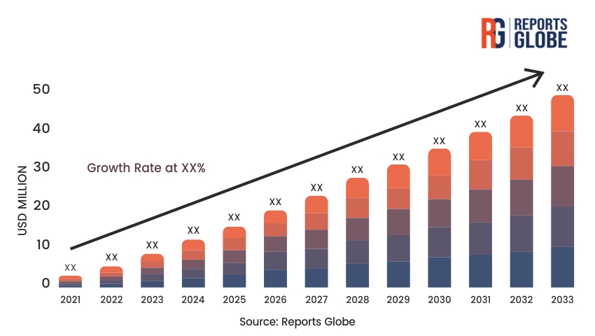
The future outlook for the bright field wafer defect inspection system market is optimistic, driven by technological advancements, increasing semiconductor production capacities, and rising demand for high-performance electronic devices. Market growth will be sustained by the proliferation of IoT devices, automotive electronics, and next-generation communication networks that require superior semiconductor quality and reliability. Furthermore, the integration of AI-driven defect inspection solutions and the adoption of advanced packaging technologies are expected to redefine the landscape of semiconductor manufacturing. Continued investments in R&D, expansion into emerging markets, and strategic collaborations will be crucial in shaping the market’s trajectory and enabling semiconductor manufacturers to maintain competitive advantage in a rapidly evolving industry landscape.
Market Segmentation
- By Type of Inspection System:
- Automated Bright Field Wafer Inspection Systems
- Semi-Automated Bright Field Wafer Inspection Systems
- By Application:
- Silicon Wafers
- Compound Semiconductor Wafers
- Others
- By End-User:
- Semiconductor Manufacturers
- Foundries
- Others
- By Region:
- North America
- Europe
- Asia-Pacific
- Latin America
- Middle East & Africa


