Automatic Wafer Defect Inspection System Market Size, Share, Growth, Trends, Statistics Analysis Report and By Segment Forecasts 2024 to 2033

Market Overview

The Automatic Wafer Defect Inspection System market has witnessed significant growth owing to advancements in semiconductor manufacturing and the increasing demand for defect-free wafers in electronics and semiconductor industries. These systems play a crucial role in detecting and categorizing defects on semiconductor wafers with high precision and speed. With the semiconductor industry’s continuous push towards miniaturization and higher integration densities, the need for reliable defect inspection systems has become paramount. Automatic wafer defect inspection systems utilize advanced technologies such as machine vision, artificial intelligence (AI), and deep learning algorithms to identify defects at various stages of semiconductor production, ensuring high yield and quality. The market is characterized by rapid technological advancements, strategic collaborations, and increasing investments in research and development (R&D) to enhance inspection capabilities.
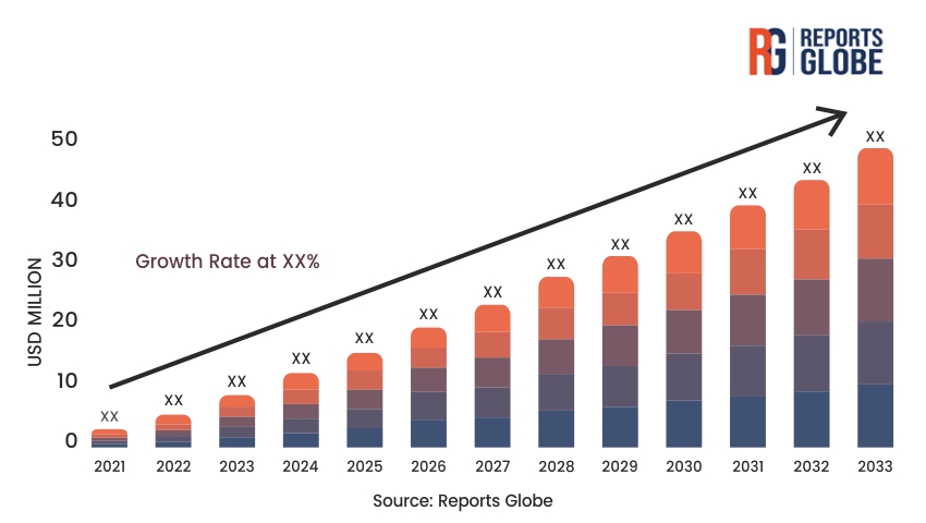
Key Takeaways of the Market

  • Increasing adoption of automatic wafer defect inspection systems in semiconductor fabrication facilities worldwide.
  • Technological advancements in machine vision and AI algorithms are driving system accuracy and efficiency.
  • Growing demand for defect-free wafers to meet stringent quality standards in semiconductor manufacturing.
  • Asia-Pacific region dominates the market due to the presence of major semiconductor manufacturers and increasing investments in semiconductor production facilities.
  • Integration of automatic defect inspection systems with smart manufacturing initiatives to optimize production processes.

Market Driver

The primary driver of the Automatic Wafer Defect Inspection System market is the relentless pursuit of higher semiconductor yield and quality. As semiconductor manufacturers strive to produce smaller, more complex chips with higher integration densities, the risk of defects increases proportionally. Automatic wafer defect inspection systems address this challenge by providing comprehensive defect detection capabilities across various stages of semiconductor fabrication. These systems leverage advanced imaging technologies and sophisticated algorithms to identify defects such as particles, scratches, pattern deviations, and electrical faults with unmatched precision and speed.

Moreover, the shift towards advanced packaging technologies such as 3D ICs and wafer-level packaging further underscores the importance of robust defect inspection systems. These technologies demand stringent quality control measures to ensure reliability and performance, driving the adoption of automatic defect inspection solutions. Additionally, the integration of AI and machine learning algorithms enables continuous improvement in defect detection accuracy and the ability to analyze large volumes of data generated during inspection processes. As semiconductor manufacturers strive to maintain competitive edge and meet evolving market demands, automatic wafer defect inspection systems remain indispensable in achieving high yield and optimizing production efficiency.

Market Restraint

Despite the growth prospects, the Automatic Wafer Defect Inspection System market faces challenges, including high initial investment costs and complexity of system integration. Implementing automatic defect inspection systems requires substantial capital expenditure, particularly for advanced models capable of handling high-resolution imaging and complex data processing tasks. This poses a barrier to adoption, particularly for small and medium-sized semiconductor manufacturers with limited financial resources.

Furthermore, the complexity of semiconductor manufacturing processes and the diversity of defect types present technical challenges in developing universal defect detection algorithms. Variations in materials, patterns, and structures across different semiconductor devices necessitate customized inspection solutions, adding to the complexity and cost. Moreover, the rapid pace of technological advancements requires continuous upgrades and maintenance of inspection systems to keep pace with industry standards, further adding to the total cost of ownership. These factors collectively restrain market growth and hinder the widespread adoption of automatic wafer defect inspection systems.

Market Opportunity

The Automatic Wafer Defect Inspection System market presents significant opportunities, particularly with the advent of advanced semiconductor technologies and emerging applications. One of the key opportunities lies in the development of next-generation inspection systems capable of addressing the challenges posed by new materials and structures in semiconductor manufacturing. Innovations in imaging technologies, including hyperspectral imaging and advanced microscopy techniques, offer new avenues for enhancing defect detection capabilities and expanding the application scope of automatic inspection systems.

Moreover, the increasing adoption of Internet of Things (IoT) and smart manufacturing initiatives presents opportunities for integrating defect inspection systems with broader manufacturing ecosystems. By leveraging real-time data analytics and predictive maintenance capabilities, manufacturers can optimize production processes, reduce downtime, and improve overall efficiency. The demand for defect inspection systems is also expected to surge with the proliferation of applications such as automotive electronics, consumer electronics, and medical devices, where semiconductor reliability and quality are critical.

Market Segment Analysis

Semiconductor Foundries

Automatic wafer defect inspection systems find extensive use in semiconductor foundries, where they are employed to ensure the quality and reliability of wafers throughout the manufacturing process. Foundries require high-throughput inspection systems capable of detecting defects at micron-level resolutions to maintain high yield rates. These systems play a crucial role in identifying defects such as lithography errors, contamination, and electrical faults, thereby minimizing production losses and enhancing overall process efficiency. The demand for automatic defect inspection systems in semiconductor foundries is driven by the increasing complexity of semiconductor designs and the need for stringent quality control measures.

Integrated Device Manufacturers (IDMs)

Integrated Device Manufacturers (IDMs) represent another significant segment for automatic wafer defect inspection systems. IDMs typically operate their semiconductor fabrication facilities and require comprehensive defect inspection solutions to ensure the quality and reliability of their integrated circuits (ICs). These systems are integrated into various stages of IC manufacturing, including wafer probing, lithography, and packaging, to detect defects that could impact device performance or reliability. The growing adoption of advanced packaging technologies and the shift towards smaller node sizes further amplify the demand for high-precision defect inspection systems among IDMs.

Regional Analysis

The Automatic Wafer Defect Inspection System market exhibits distinct regional dynamics, influenced by factors such as semiconductor manufacturing prowess, technological innovation, and regulatory environments.

Asia-Pacific dominates the global market, driven by the presence of major semiconductor manufacturing hubs in countries like China, Taiwan, South Korea, and Japan. These nations host some of the world’s largest semiconductor foundries and integrated device manufacturers (IDMs), contributing significantly to market growth. The region benefits from extensive investments in semiconductor production facilities, favorable government policies supporting semiconductor industries, and a robust ecosystem of equipment suppliers and technology providers. Moreover, the rapid expansion of consumer electronics, automotive electronics, and industrial automation sectors in Asia-Pacific fuels the demand for advanced defect inspection systems, thereby driving market expansion further.

North America and Europe also hold substantial market shares, characterized by technological leadership, stringent quality standards, and significant investments in research and development. In North America, the presence of leading semiconductor companies and advanced technological capabilities in AI, machine learning, and imaging technologies drive market growth. The region focuses on innovation and product development, leveraging strategic collaborations between industry players and academic institutions. Similarly, Europe emphasizes sustainable manufacturing practices and regulatory compliance, influencing the adoption of automatic defect inspection systems across semiconductor manufacturing facilities.

Latin America, Middle East, and Africa are emerging regions in the market, witnessing gradual adoption of automatic defect inspection systems. These regions benefit from increasing investments in infrastructure development and expanding electronics manufacturing sectors. However, market growth is constrained by economic volatility, technological infrastructure limitations, and comparatively lower levels of semiconductor manufacturing activity. Nonetheless, strategic partnerships and government initiatives promoting technology adoption are expected to spur market growth in these regions over the forecast period.

Competitive Analysis

The Automatic Wafer Defect Inspection System market is highly competitive, characterized by intense rivalry among global and regional players striving for technological innovation and market leadership. Key players such as KLA Corporation, Applied Materials, Inc., and Nanometrics Incorporated dominate the market with their extensive product portfolios and established customer base in semiconductor manufacturing. These companies invest significantly in research and development to develop advanced defect inspection technologies capable of meeting stringent industry requirements.

Strategic collaborations and partnerships are prevalent strategies among market players, aimed at enhancing technological capabilities and expanding market reach. Collaborations with semiconductor manufacturers, research institutions, and technology providers facilitate the development of next-generation defect inspection solutions. Moreover, mergers and acquisitions play a crucial role in market consolidation, enabling companies to strengthen their technological competencies and leverage synergies in product development and innovation.

The competitive landscape is also characterized by continuous product enhancements and customer-centric approaches. Companies focus on developing customized defect inspection solutions tailored to specific application needs across semiconductor foundries, IDMs, and outsourced semiconductor assembly and test (OSAT) companies. Additionally, the integration of artificial intelligence (AI) and machine learning algorithms into defect inspection systems enables real-time defect classification and predictive maintenance capabilities, further enhancing system performance and operational efficiency.

Looking forward, market players are expected to intensify their efforts in technological innovation and strategic partnerships to capitalize on emerging opportunities in advanced packaging technologies, IoT integration, and smart manufacturing initiatives. The emphasis on sustainable manufacturing practices and regulatory compliance will also shape competitive strategies, as companies aim to differentiate themselves through superior product quality, reliability, and customer satisfaction in the global Automatic Wafer Defect Inspection System market.

Key Industry Developments

  • Introduction of advanced automatic wafer defect inspection systems with AI and machine learning capabilities.
  • Strategic collaborations between technology providers and semiconductor manufacturers to enhance defect detection accuracy.
  • Development of high-throughput defect inspection solutions for semiconductor foundries and IDMs.
  • Integration of IoT and smart manufacturing initiatives with defect inspection systems to optimize production processes.
  • Adoption of advanced imaging technologies, including hyperspectral imaging and advanced microscopy, for enhanced defect detection capabilities.
  • Expansion of production capacities and service capabilities to meet the growing demand for defect inspection systems globally.
  • Focus on developing customized defect inspection solutions for emerging applications such as automotive electronics and medical devices.
  • Implementation of predictive maintenance and remote monitoring capabilities in defect inspection systems to minimize downtime and improve operational efficiency.
  • Introduction of cloud-based defect analysis platforms for real-time data analytics and decision-making in semiconductor manufacturing.
  • Continuous investments in R&D to address the challenges posed by new materials and structures in semiconductor fabrication.

Future Outlook

The Automatic Wafer Defect Inspection System market is poised for continued growth, driven by advancements in semiconductor technologies, increasing demand for high-quality semiconductor products, and the proliferation of smart manufacturing initiatives. The market is expected to witness further integration of AI and machine learning algorithms into defect inspection systems, enabling real-time defect classification and predictive maintenance capabilities. Moreover, the development of compact, high-resolution imaging technologies will enhance system performance and expand application possibilities across various industries.

The demand for automatic defect inspection systems is projected to grow with the rising adoption of advanced packaging technologies, including 3D ICs and wafer-level packaging, which require stringent quality control measures. Additionally, the expansion of semiconductor manufacturing capabilities in emerging economies and the increasing penetration of electronic devices in automotive and industrial sectors will fuel market growth. Strategic partnerships and collaborations will play a crucial role in driving innovation and expanding market reach, enabling companies to capitalize on emerging opportunities and maintain competitive advantage in the global semiconductor landscape.

Market Segmentation

  • By Type
    • Optical Inspection Systems
    • Electron Beam Inspection Systems
    • Laser Scanning Inspection Systems
  • By Application
    • Wafer Inspection
    • Mask Inspection
    • Metrology
  • By End-Use Industry
    • Semiconductor Foundries
    • Integrated Device Manufacturers (IDMs)
    • Outsourced Semiconductor Assembly and Test (OSAT) Companies
  • By Region
    • North America
    • Europe
    • Asia-Pacific
    • Latin America
    • Middle East and Africa

Table of Contents

Chapter 1. Research Methodology & Data Sources

1.1. Data Analysis Models
1.2. Research Scope & Assumptions
1.3. List of Primary & Secondary Data Sources 

Chapter 2. Executive Summary

2.1. Market Overview
2.2. Segment Overview
2.3. Market Size and Estimates, 2021 to 2033
2.4. Market Size and Estimates, By Segments, 2021 to 2033

Chapter 3. Industry Analysis

3.1. Market Segmentation
3.2. Market Definitions and Assumptions
3.3. Supply chain analysis
3.4. Porter’s five forces analysis
3.5. PEST analysis
3.6. Market Dynamics
3.6.1. Market Driver Analysis
3.6.2. Market Restraint analysis
3.6.3. Market Opportunity Analysis
3.7. Competitive Positioning Analysis, 2023
3.8. Key Player Ranking, 2023

Chapter 4. Market Segment Analysis- Segment 1

4.1.1. Historic Market Data & Future Forecasts, 2024-2033
4.1.2. Historic Market Data & Future Forecasts by Region, 2024-2033

Chapter 5. Market Segment Analysis- Segment 2

5.1.1. Historic Market Data & Future Forecasts, 2024-2033
5.1.2. Historic Market Data & Future Forecasts by Region, 2024-2033

Chapter 6. Regional or Country Market Insights

** Reports focusing on a particular region or country will contain data unique to that region or country **

6.1. Global Market Data & Future Forecasts, By Region 2024-2033

6.2. North America
6.2.1. Historic Market Data & Future Forecasts, 2024-2033
6.2.2. Historic Market Data & Future Forecasts, By Segment 1, 2024-2033
6.2.3. Historic Market Data & Future Forecasts, By Segment 2, 2024-2033

6.2.4. U.S.
6.2.4.1. Historic Market Data & Future Forecasts, 2024-2033
6.2.4.2. Historic Market Data & Future Forecasts, By Segment 1, 2024-2033
6.2.4.3. Historic Market Data & Future Forecasts, By Segment 2, 2024-2033

6.2.5. Canada
6.2.5.1. Historic Market Data & Future Forecasts, 2024-2033
6.2.5.2. Historic Market Data & Future Forecasts, By Segment 1, 2024-2033
6.2.5.3. Historic Market Data & Future Forecasts, By Segment 2, 2024-2033

6.3. Europe
6.3.1. Historic Market Data & Future Forecasts, 2024-2033
6.3.2. Historic Market Data & Future Forecasts, By Segment 1, 2024-2033
6.3.3. Historic Market Data & Future Forecasts, By Segment 2, 2024-2033

6.3.4. UK
6.3.4.1. Historic Market Data & Future Forecasts, 2024-2033
6.3.4.2. Historic Market Data & Future Forecasts, By Segment 1, 2024-2033
6.3.4.3. Historic Market Data & Future Forecasts, By Segment 2, 2024-2033

6.3.5. Germany
6.3.5.1. Historic Market Data & Future Forecasts, 2024-2033
6.3.5.2. Historic Market Data & Future Forecasts, By Segment 1, 2024-2033
6.3.5.3. Historic Market Data & Future Forecasts, By Segment 2, 2024-2033

6.3.6. France
6.3.6.1. Historic Market Data & Future Forecasts, 2024-2033
6.3.6.2. Historic Market Data & Future Forecasts, By Segment 1, 2024-2033
6.3.6.3. Historic Market Data & Future Forecasts, By Segment 2, 2024-2033

6.4. Asia Pacific
6.4.1. Historic Market Data & Future Forecasts, 2024-2033
6.4.2. Historic Market Data & Future Forecasts, By Segment 1, 2024-2033
6.4.3. Historic Market Data & Future Forecasts, By Segment 2, 2024-2033

6.4.4. China
6.4.4.1. Historic Market Data & Future Forecasts, 2024-2033
6.4.4.2. Historic Market Data & Future Forecasts, By Segment 1, 2024-2033
6.4.4.3. Historic Market Data & Future Forecasts, By Segment 2, 2024-2033

6.4.5. India
6.4.5.1. Historic Market Data & Future Forecasts, 2024-2033
6.4.5.2. Historic Market Data & Future Forecasts, By Segment 1, 2024-2033
6.4.5.3. Historic Market Data & Future Forecasts, By Segment 2, 2024-2033

6.4.6. Japan
6.4.6.1. Historic Market Data & Future Forecasts, 2024-2033
6.4.6.2. Historic Market Data & Future Forecasts, By Segment 1, 2024-2033
6.4.6.3. Historic Market Data & Future Forecasts, By Segment 2, 2024-2033

6.4.7. South Korea
6.4.7.1. Historic Market Data & Future Forecasts, 2024-2033
6.4.7.2. Historic Market Data & Future Forecasts, By Segment 1, 2024-2033
6.4.7.3. Historic Market Data & Future Forecasts, By Segment 2, 2024-2033

6.5. Latin America
6.5.1. Historic Market Data & Future Forecasts, 2024-2033
6.5.2. Historic Market Data & Future Forecasts, By Segment 1, 2024-2033
6.5.3. Historic Market Data & Future Forecasts, By Segment 2, 2024-2033

6.5.4. Brazil
6.5.4.1. Historic Market Data & Future Forecasts, 2024-2033
6.5.4.2. Historic Market Data & Future Forecasts, By Segment 1, 2024-2033
6.5.4.3. Historic Market Data & Future Forecasts, By Segment 2, 2024-2033

6.5.5. Mexico
6.5.5.1. Historic Market Data & Future Forecasts, 2024-2033
6.5.5.2. Historic Market Data & Future Forecasts, By Segment 1, 2024-2033
6.5.5.3. Historic Market Data & Future Forecasts, By Segment 2, 2024-2033

6.6. Middle East & Africa
6.6.1. Historic Market Data & Future Forecasts, 2024-2033
6.6.2. Historic Market Data & Future Forecasts, By Segment 1, 2024-2033
6.6.3. Historic Market Data & Future Forecasts, By Segment 2, 2024-2033

6.6.4. UAE
6.6.4.1. Historic Market Data & Future Forecasts, 2024-2033
6.6.4.2. Historic Market Data & Future Forecasts, By Segment 1, 2024-2033
6.6.4.3. Historic Market Data & Future Forecasts, By Segment 2, 2024-2033

6.6.5. Saudi Arabia
6.6.5.1. Historic Market Data & Future Forecasts, 2024-2033
6.6.5.2. Historic Market Data & Future Forecasts, By Segment 1, 2024-2033
6.6.5.3. Historic Market Data & Future Forecasts, By Segment 2, 2024-2033

6.6.6. South Africa
6.6.6.1. Historic Market Data & Future Forecasts, 2024-2033
6.6.6.2. Historic Market Data & Future Forecasts, By Segment 1, 2024-2033
6.6.6.3. Historic Market Data & Future Forecasts, By Segment 2, 2024-2033

Chapter 7. Competitive Landscape

7.1. Competitive Heatmap Analysis, 2023
7.2. Competitive Product Analysis

7.3. Company 1
7.3.1. Company Description
7.3.2. Financial Highlights
7.3.3. Product Portfolio
7.3.4. Strategic Initiatives

7.4. Company 2
7.4.1. Company Description
7.4.2. Financial Highlights
7.4.3. Product Portfolio
7.4.4. Strategic Initiatives

7.5. Company 3
7.5.1. Company Description
7.5.2. Financial Highlights
7.5.3. Product Portfolio
7.5.4. Strategic Initiatives

7.6. Company 4
7.6.1. Company Description
7.6.2. Financial Highlights
7.6.3. Product Portfolio
7.6.4. Strategic Initiatives

7.7. Company 5
7.7.1. Company Description
7.7.2. Financial Highlights
7.7.3. Product Portfolio
7.7.4. Strategic Initiatives

7.8. Company 6
7.8.1. Company Description
7.8.2. Financial Highlights
7.8.3. Product Portfolio
7.8.4. Strategic Initiatives

7.9. Company 7
7.9.1. Company Description
7.9.2. Financial Highlights
7.9.3. Product Portfolio
7.9.4. Strategic Initiatives

7.10. Company 8
7.10.1. Company Description
7.10.2. Financial Highlights
7.10.3. Product Portfolio
7.10.4. Strategic Initiatives

7.11. Company 9
7.11.1. Company Description
7.11.2. Financial Highlights
7.11.3. Product Portfolio
7.11.4. Strategic Initiatives

7.12. Company 10
7.12.1. Company Description
7.12.2. Financial Highlights
7.12.3. Product Portfolio
7.12.4. Strategic Initiatives

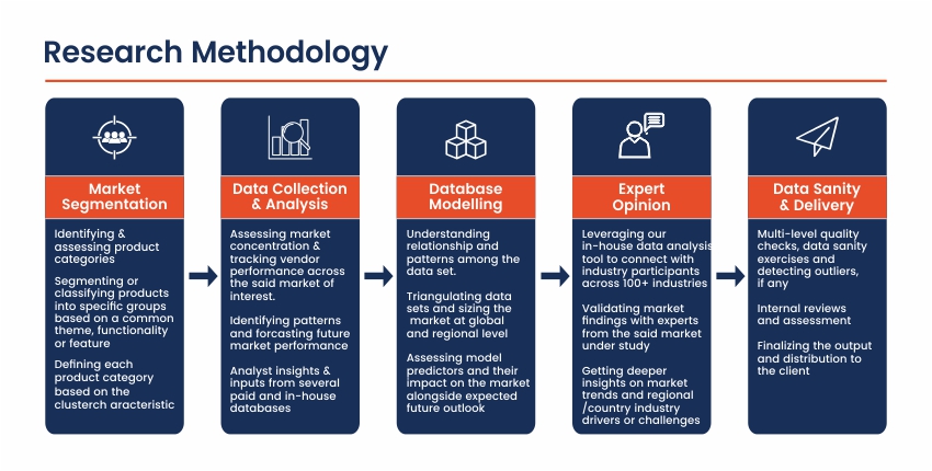
Research Methodology

Frequently Asked Questions About This Report

Choose License Type

$3,240
$3,780
$4,410

Our salient features

Best Solution

We will assist you in comprehending the value propositions of various reports across multiple domains and recommend the optimal solution to meet your research requirements.

Customized Research

Our team of analysts and consultants provide assistance for customized research requirements

Max ROI

Guaranteed maximum assistance to help you get your reports at the optimum prices, thereby ensuring maximum returns on investment.

24/7 Support

24X7 availability to help you through the buying process as well as answer any of your doubts.

Get a free sample report

This free sample study provides a comprehensive overview of the report, including an executive summary, market segments, complete analysis, country-level analysis, and more.

Our Clients

We've Received Your Request

We Thank You for filling out your requirements. Our sales team will get in touch with you shortly.